

 English
 中文简体
中文简体 Español
 عربى
عربىPCB Pad Layout and Via Design for BTB Connectors
Introduction to PCB Design for BTB Connectors
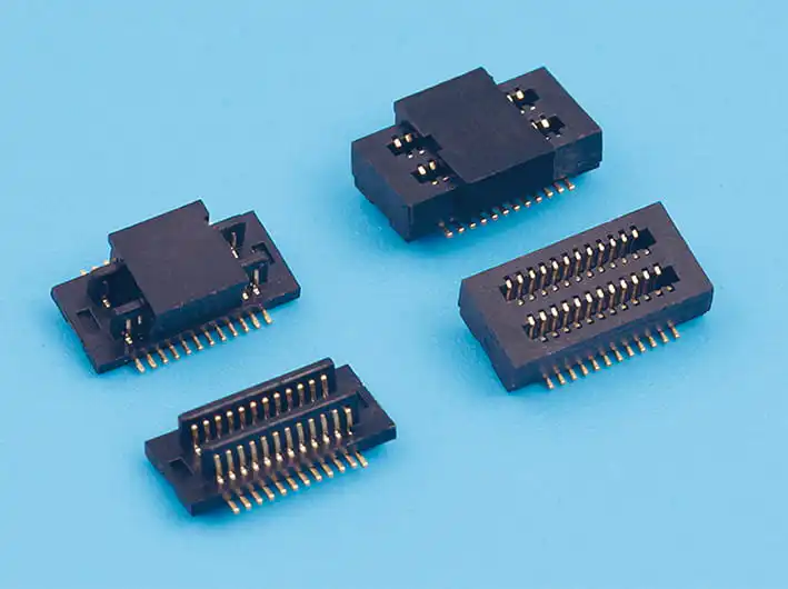
The BTB Connector plays a critical role in providing reliable board-to-board power and signal connections. Proper PCB design is essential to ensure electrical performance, mechanical stability, and long-term reliability. Inadequate pad layout or via placement can cause solder joint failures, increased impedance, or mechanical stress issues.
Pad Layout Considerations
- Pad Size and Shape: The pad dimensions must match the connector’s terminal size while providing enough surface area for soldering. Larger pads improve solder joint strength but can increase the risk of solder bridging, especially for high-density connectors. Rectangular or oval pad shapes are often preferred for power pins to increase current-carrying capacity.
- Pad Spacing: Maintain proper clearance between adjacent pads to prevent solder shorts and facilitate inspection. Following the manufacturer’s recommended pitch ensures reliable assembly and reduces defects. For high-current applications, slightly increasing pad spacing can help improve thermal dissipation.
- Thermal Relief Pads: For through-hole or high-power connectors, thermal relief pads can improve soldering consistency by controlling heat flow. These pads allow even solder reflow while preventing excessive heat loss through large copper planes.
Via Design Considerations
- Via Size and Type: Vias can be used to connect top and bottom copper layers or for thermal management. The diameter of the via should balance current-carrying requirements and manufacturability. Microvias may be suitable for high-density designs, while standard plated-through holes are preferred for higher currents.
- Via Placement: Position vias carefully to avoid interfering with the connector pads. For power pins, multiple vias can help conduct heat away and reduce electrical resistance. Keep a distance from pad edges to prevent solder wicking or pad lifting during reflow.
- Via-in-Pad Technique: In some high-performance designs, placing vias directly in the pad can improve thermal and electrical performance. However, via-in-pad requires careful filling or plating to avoid solder voids and ensure mechanical stability.
Signal Integrity and Thermal Management
- Maintaining Trace Width: Trace width connecting to BTB Connector pads should be calculated based on current requirements to reduce voltage drop and resistive heating. Wider traces also help reduce inductance and signal loss for high-speed signals.
- Reducing Parasitic Effects: Keep the pad and via geometry optimized to reduce parasitic capacitance and inductance, especially for connectors handling high-frequency signals. Avoid unnecessary stubs or long via chains that can introduce signal reflection.
- Thermal Dissipation: For connectors carrying substantial current, copper pours and multiple vias can help dissipate heat. Connect pads to internal planes to spread thermal energy and prevent hot spots that may damage the PCB or connector.
Manufacturing and Assembly Considerations
Solder Mask Design: Apply solder mask between pads to prevent bridging during reflow. For high-density BTB connectors, precise mask definition is essential to maintain solder integrity.
Stencil Design: Ensure the solder paste stencil aperture matches the pad size to provide sufficient solder volume without excessive buildup. Uniform paste deposition is crucial for joint reliability.
Mechanical Support: In addition to electrical design, consider mechanical support for the connector. Larger pads and multiple vias can improve retention strength, especially for connectors subjected to repeated mating cycles.
Designing PCB pads and vias for BTB Connectors requires careful consideration of electrical, thermal, and mechanical factors. Proper pad size, spacing, and shape ensure strong solder joints, while well-planned via placement enhances current capacity and heat dissipation. By following these design principles, engineers can achieve reliable, manufacturable, and high-performance board-to-board connections that meet both signal and power requirements. Attention to these details during PCB design reduces assembly defects, improves long-term reliability, and ensures suitable connector performance.
Related Products
-

Easy-on fpc flat ribbon connector, 0.3mm pitch, 1.0mm height, flexible printed circuit connector, horizontal smt type
-

Back flip fpc flat flexible cable connector, 0.3mm pitch, 1.0mm height, bottom contact type for pcb board connections
-

Back flip micro fpc flat cable connector, 0.5mm pitch, 1.0mm height, compact design, white, for data, signal transfer applications
-

0.5mm Pitch, 1.0mm Height, Flip-Type Horizontal FPC Connector
-

0.5mm pitch 1.2mm fpc flat cable connectors, horizontal smt type, flexible printed circuit connectors, secure locking
-

0.5mm Pitch, 1.2mm Height, Rear-Entry Horizontal FPC Connector
-

0.5mm pitch 1.2mm height fpc flat cable connector, zif r/a upper contact, locking slider, high-density integration, durable, for flexible printed circuits
-

0.5mm pitch 1.2mm height fpc flat flexible cable connector, zif r/a down contact, for electronics and pcb boards
-

High-quality 0.5mm pitch 1.5mm height easy-on flat flexible cable fpc connector, horizontal type, locking-style, for pcb circuit board
-

0.5mm pitch 1.5mm height back flip fpc flat connectors, zif slide type, flexible printed circuit cable connectors, horizontal contact
-

0.5mm pitch easy-on fpc flat ribbon connector, 2.0mm height, locking zif slide type, horizontal contact, flexible printed circuit board connector
-

0.5mm pitch 2.0mm height, easy-on r/a with buckle fpc flat connectors, high-density integration flexible printed circuit board connectors
-

0.5mm Pitch, 2.0mm Height, Hinged Cover, Horizontal Mounting, Large Solder Pads
-

0.5mm pitch 2.0mm height back flip fpc flat connectors, horizontal insert, locking type, zif slide, pcb mount
-
")
0.5mm Pitch, Ultra-Thin 2.0mm Horizontal FPC Connector (Pull-Out Locking Type, Top Contact Type)
-
")
0.5mm Pitch, Ultra-Thin 2.0mm Horizontal FPC Connector (Pull-Out Locking Type, Bottom Contact Type)
-

0.5mm pitch 4.5mm height fpc flat cable connector, zif s/t reversed pointer, locking slide
-

Double-side drawing fpc flat connector, 0.5mm pitch, 2.0mm/2.5mm height, flip type, for flexible cable, pcb mountable
CONTACT INFORMATION
-
Mr.Zhou(Sales manager)
Tel:+86(0)577-62369959
Tel:+86(0)577-62378959
MP:+86-13570877599
E-mail:[email protected]
Wechat:+86-13570877599
PRODUCT LINKS

Copyright © Zhejiang Wenda Electronics Co., Ltd. All Rights Reserved

Custom Electronic Connectors Manufacturer
