


 English
 中文简体
 Español
 عربى
Industry News
Home / News / Industry News / How Does a Board-To-Board Connector Support High-Speed Data Transmission in Modern Electronics?
Modern electronic devices often contain several printed circuit boards (PCBs) that need to exchange data. Smartphones, servers, industrial controllers, and automotive systems are common examples. Space is limited, so separate wires between every board are rarely practical. A Board-To-Board Connector provides a compact path for signals and power.
At high data rates, the connector does more than hold two boards together. Its electrical design affects signal quality, while its size and construction must suit the product. OEM engineers need to consider both when selecting a component.
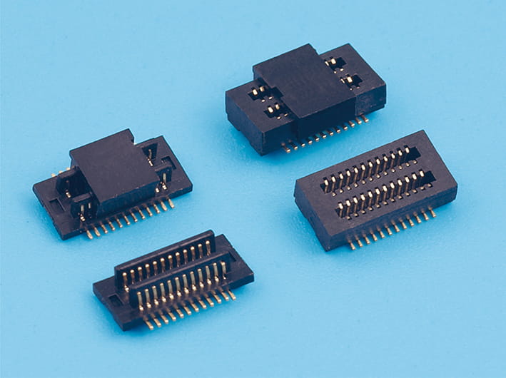
A board-to-board connector joins two PCBs through matching contacts. The boards may sit parallel to each other, connect vertically, or meet at an angle, depending on the device layout. Once mated, the contacts form conductive paths between the circuits.
High-speed signals are sensitive to small electrical changes. Fast transitions contain high-frequency components that can be affected by impedance discontinuities, parasitic capacitance, and parasitic inductance. This may cause reflections, insertion loss, crosstalk, or electromagnetic interference (EMI). Contact shape, spacing, and housing design all influence the signal as it passes through the connector.
When connector impedance differs from that of the PCB transmission line, part of the signal may reflect at the interface. Reflections can distort the waveform and reduce timing margin. Engineers should compare the connector's impedance specification with the interface requirements. Common nominal values are 50 ohms for single-ended signals and 100 ohms for differential signals, depending on the protocol.
The datasheet should also include several other electrical parameters:
Check the stated frequency range and test conditions, too. Results from different setups may not be directly comparable.
Contact geometry affects both signal behavior and connector size. Shorter contact paths can reduce parasitic effects, while suitable spacing can limit coupling between contacts. A smaller pitch allows more connections in a limited area, but leaves less room for PCB routing and manufacturing tolerances.
High-speed designs often place ground contacts alongside signal contacts to provide return-current paths and manage coupling. The return path is part of the signal circuit, so its layout matters.
| Design factor | High-speed consideration | Potential benefit |
|---|---|---|
| Contact length | Keep the signal path short | Reduces parasitic effects |
| Contact pitch | Balance density with electrical spacing | Helps control crosstalk |
| Ground contacts | Provide suitable return-current paths | Supports signal integrity |
| Impedance design | Match the PCB transmission line | Reduces reflections |
| Shielding | Use where EMI control is needed | Limits electromagnetic coupling |
| Connector height | Check board spacing and clearance | Supports the required PCB stack-up |
A dense connector is not automatically a better high-speed option. The contact layout and its connection to the PCB determine the result.
The connector cannot be assessed on its own. A poor PCB breakout can undermine its electrical performance. Keep traces between the connector and nearby components short where possible, and maintain consistent spacing through differential-pair breakout areas.
The ground plane should provide a continuous return path. Gaps in the reference plane, unused vias, sudden trace-width changes, and poorly placed ground connections can add discontinuities. Pin assignment matters as well: ground contacts between groups of high-speed signals can help limit coupling.
For demanding designs, engineers can use electromagnetic simulation and confirm the results with time-domain or frequency-domain measurements. Tests should reflect the actual PCB stack-up and routing.
The connection must also hold up under real operating conditions. Vibration, shock, temperature changes, and repeated mating can affect contact reliability. Check retention force, rated mating cycles, operating temperature, and allowable misalignment against the intended use.
Gold-plated contacts are common where reliable electrical contact is required. Plating thickness and wear resistance should also suit the expected mating frequency and service environment.
Stack height is another practical detail. The connector must bridge the space between boards without interfering with components, cooling parts, or the enclosure. A poor fit can complicate assembly or put stress on the contacts.
Before approving a connector, review its datasheet and request signal-integrity results, including insertion loss, return loss, crosstalk, and impedance. Check that the test frequency and setup are relevant to the intended data rate.
Test prototypes in the actual assembly. Review signal performance, temperature behavior, mating reliability, and mechanical stability. For critical interfaces, use the intended PCB stack-up, routing, and connector arrangement rather than relying only on standalone connector data.
A Board-To-Board Connector provides the physical and electrical link between circuit boards. Its effect on high-speed transmission depends on the connector and the PCB design around it. Checking both during qualification gives OEM teams a clearer picture of how the connection will perform in the finished product.


Copyright © Zhejiang Wenda Electronics Co., Ltd. All Rights Reserved

Custom Electronic Connectors Manufacturer

